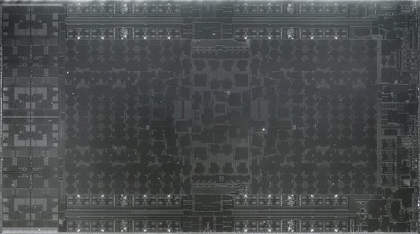
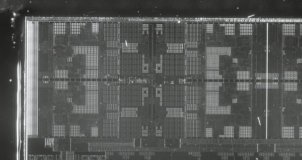
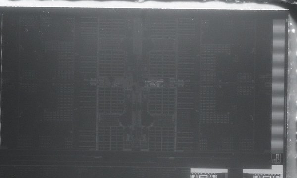
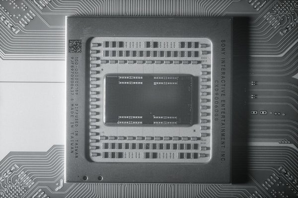
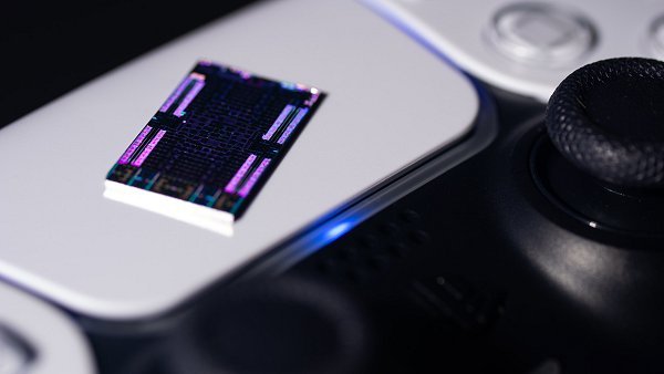
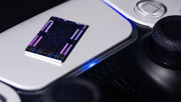
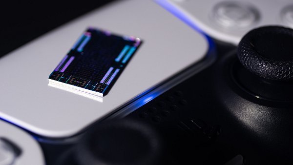
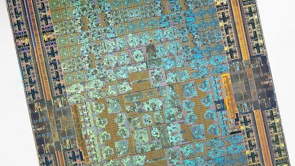
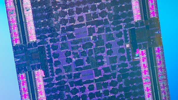
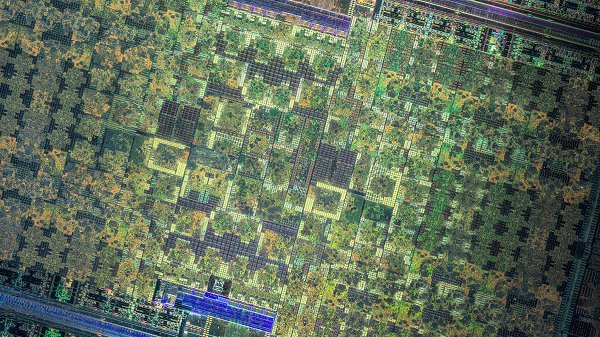
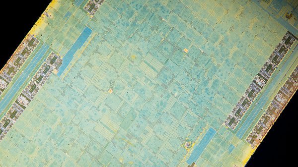
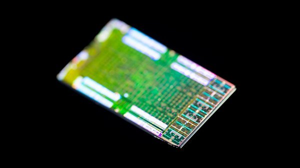
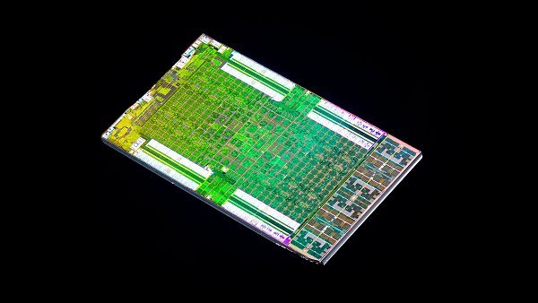
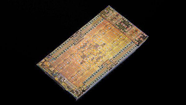
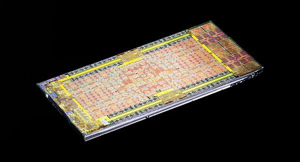
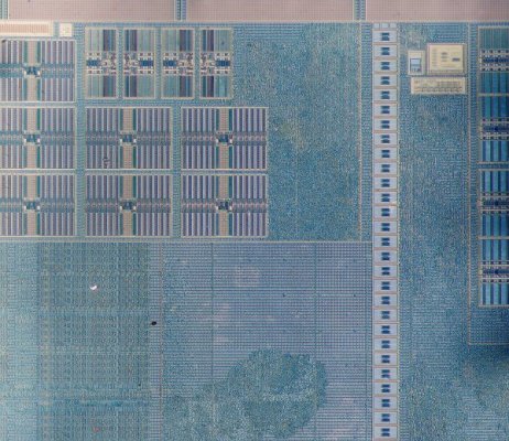
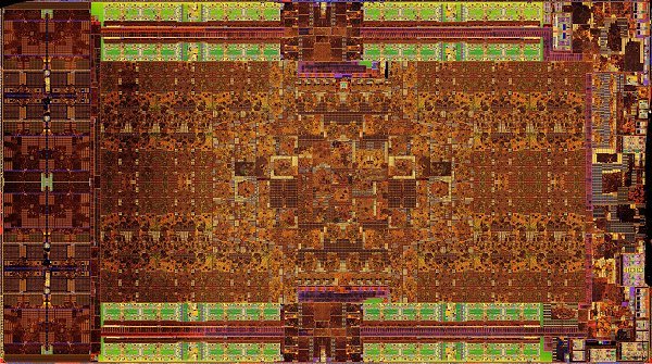
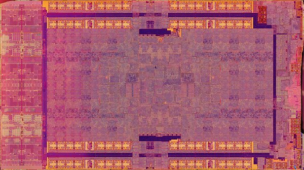
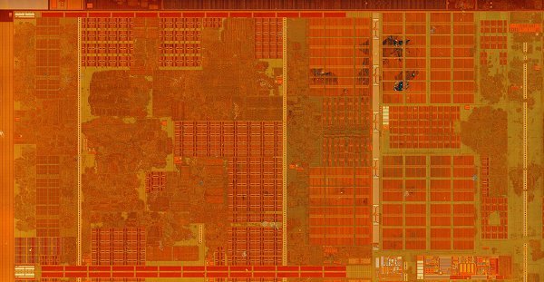
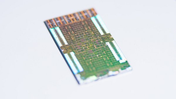
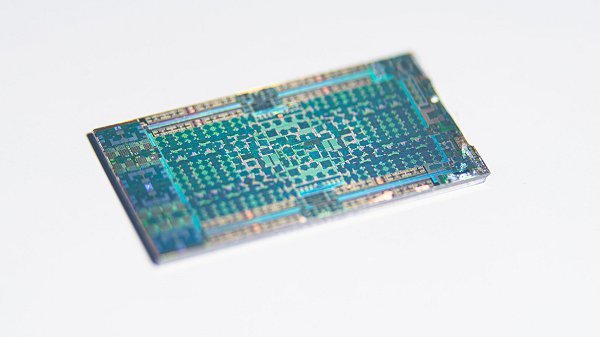
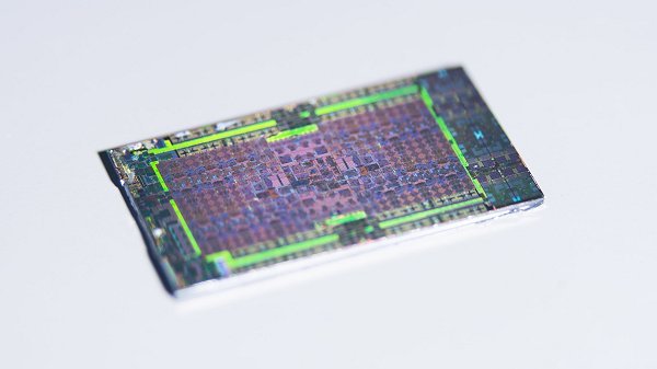
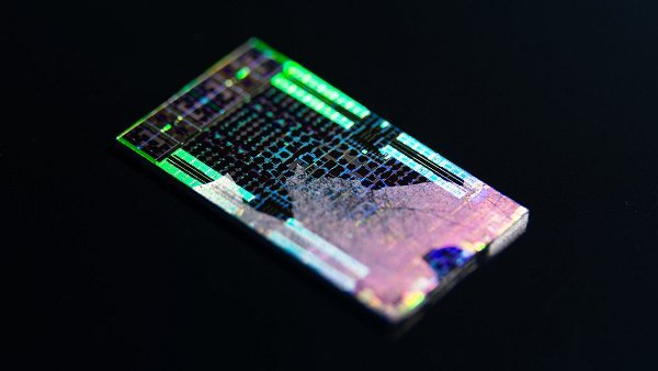
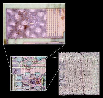
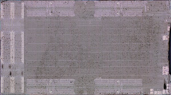
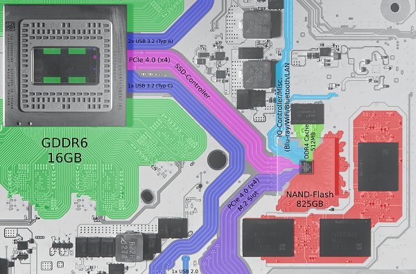
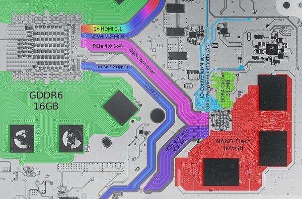
Proceeding the PS4 Syscon High-Res Images, PS4 APU Floor Plan High-Res Die Shots and his PlayStation 4 Pro photo album, recently FritzchensFritz made available some PS5 CXD90060GG SoC (System on a Chip) integrated circuit images of the PlayStation 5 silicon processor. 

Here's more details from VideoCardz.com, to quote: It has been months since PS5 was introduced, but only now we get to see a chip codenamed AMD Flute up close.
The Sony PS5 SoC codenamed known as Oberon or Ariel is based on AMD technology (Flute is AMD codename). It features both AMD Zen2 core architecture as well as RDNA2 GPU. The 8-cores Zen2 cores are clocked up to 3.5 GHz, while 36 RDNA2 Compute Units can reach a clock speed up to 2.23 GHz.
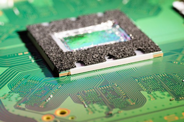
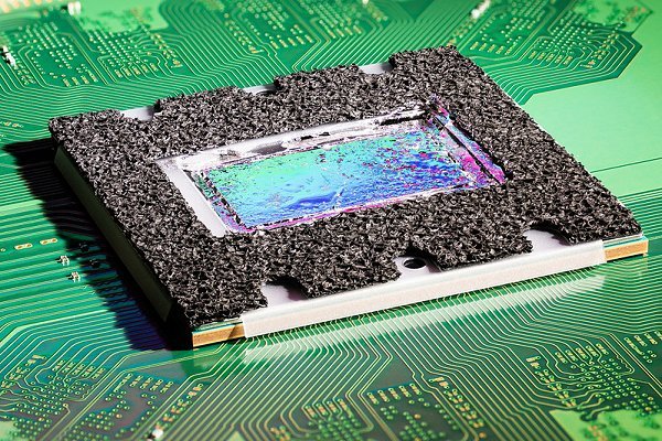
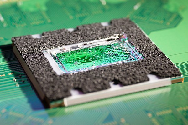
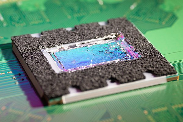
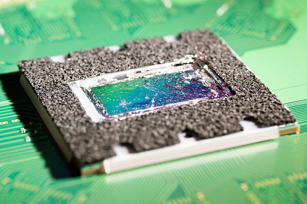
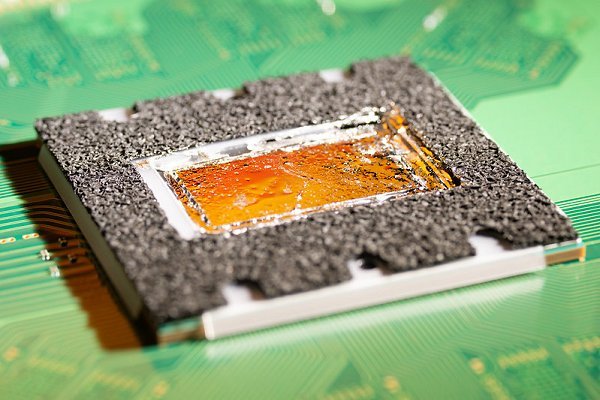
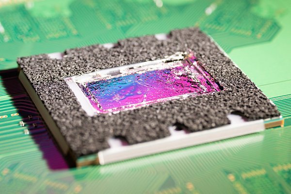
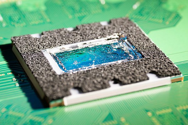
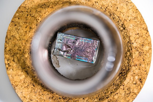
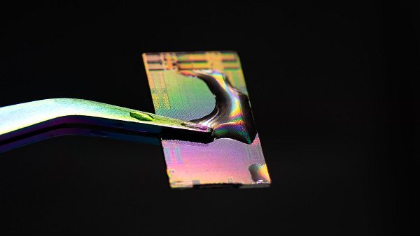
Sony announced that its PS5 chip will feature liquid metal instead of traditional thermal paste. This would ensure a longer lifespan and increase heat exchange between the chip and the cooler. However, at the same time, it increases the production complexity and forces Sony to use custom packing solutions to ensure no liquid metal spill would occur.
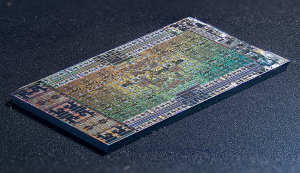
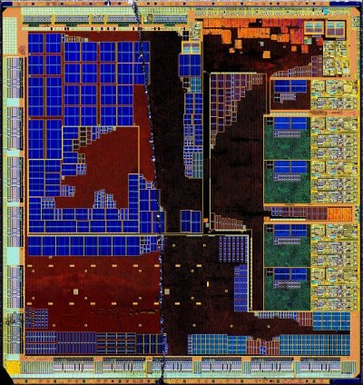
The die was pictured using a special microscope using short wave infrared light (SWIR). This technology allows the photographer to look under the hood and see the internals of the SoC without typical detaching and grinding techniques, which would also destroy the chip in the process.
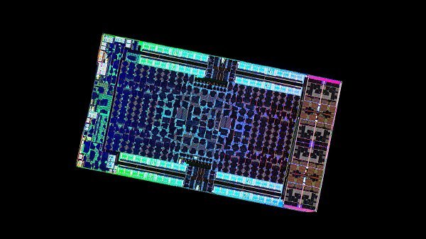
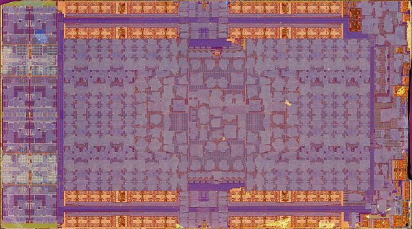
Sony PS5 chip has 8 cores located on the left side, while 36 Compute Units are packed together in a middle. The die picture confirms that the chip features eight 32-bit memory interfaces for GDDR6 memory. It also confirms that the chip has some changes to the layout compared to Zen2 based APUs.
It would appear that the chip has some Fixed Function Units (FFU) missing as well as Fused Multiply-Add (FMA/FMADD) are not be seen on the chip. Those units were likely removed as they are not required for a gaming console.
Also included in the Tweets embedded below is a a tentative die shot analysis from Locuza_, who stated the following to quote:
My interpretation of the floor plan PS5 floor plan:
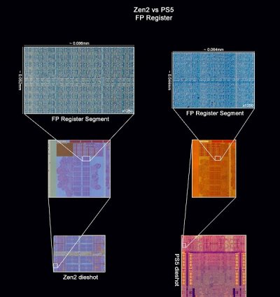
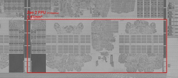
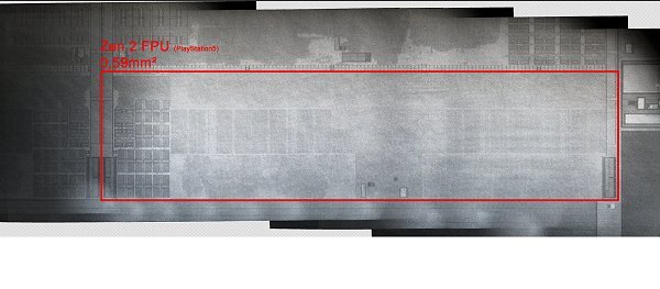
PlayStation 5 annotation of FritzchensFritz's great IR pic is here silicongang! CPU FPUs are cut-down vs normal Zen 2. GPU WGPs appear different to RDNA1's while the frontend & ROPs are similar. Also appears to support Display-over-USB, perhaps for the front USB-C for VR?
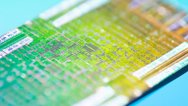
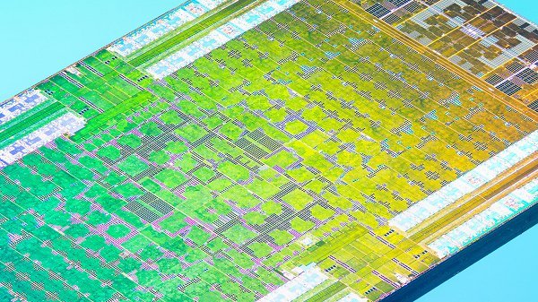
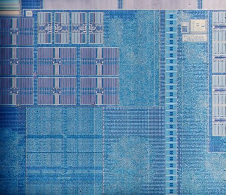
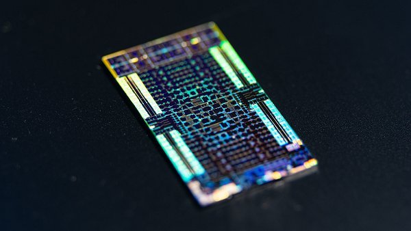
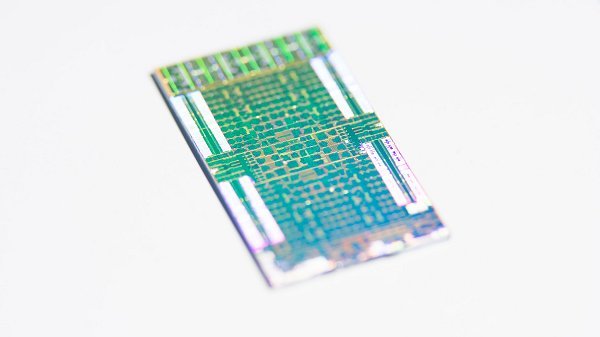
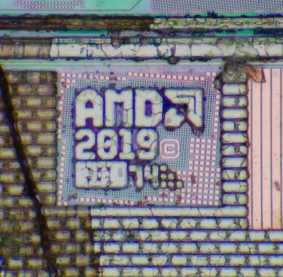
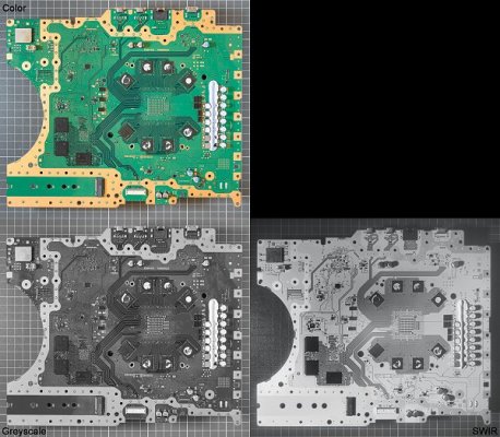
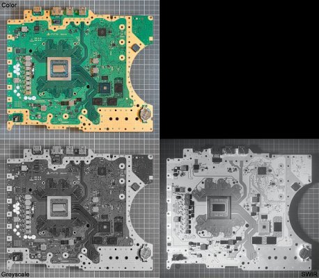
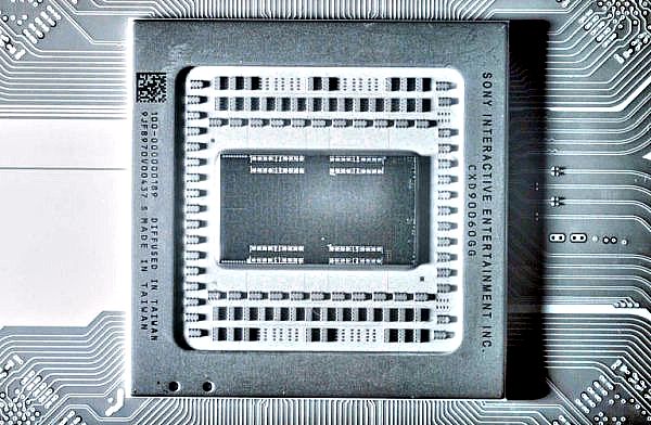
Here are some thumbnails of the PS5 Chip pictures featuring close-ups of Sony's liquid metal interface used to regulate the PS5 Temperature, and be sure to check out the high-resolution images on his PlayStation 5 Flickr gallery for some awesome PS5 Die Shots:
Here's more details from VideoCardz.com, to quote: It has been months since PS5 was introduced, but only now we get to see a chip codenamed AMD Flute up close.
The Sony PS5 SoC codenamed known as Oberon or Ariel is based on AMD technology (Flute is AMD codename). It features both AMD Zen2 core architecture as well as RDNA2 GPU. The 8-cores Zen2 cores are clocked up to 3.5 GHz, while 36 RDNA2 Compute Units can reach a clock speed up to 2.23 GHz.
Sony announced that its PS5 chip will feature liquid metal instead of traditional thermal paste. This would ensure a longer lifespan and increase heat exchange between the chip and the cooler. However, at the same time, it increases the production complexity and forces Sony to use custom packing solutions to ensure no liquid metal spill would occur.
The die was pictured using a special microscope using short wave infrared light (SWIR). This technology allows the photographer to look under the hood and see the internals of the SoC without typical detaching and grinding techniques, which would also destroy the chip in the process.
Sony PS5 chip has 8 cores located on the left side, while 36 Compute Units are packed together in a middle. The die picture confirms that the chip features eight 32-bit memory interfaces for GDDR6 memory. It also confirms that the chip has some changes to the layout compared to Zen2 based APUs.
It would appear that the chip has some Fixed Function Units (FFU) missing as well as Fused Multiply-Add (FMA/FMADD) are not be seen on the chip. Those units were likely removed as they are not required for a gaming console.
Also included in the Tweets embedded below is a a tentative die shot analysis from Locuza_, who stated the following to quote:
My interpretation of the floor plan PS5 floor plan:
- Bomba surprise that Sony likely cut down the 256-Bit FP pipes to just 128-Bit.
- No Infinity Cache/L3$, also not on the Xbox Series.
- Might have the old Render Backend design, need higher res to say for sure.
- The WGPs are arranged as on RDNA1 GPUs with two sub-arrays. Same goes for the Xbox Series. Navi21/22/23, Van Gogh and Rembrandt only have one sub-array for all WGPs.
- Higher res needed for a closer FPU look, GPU frontend analysis and details like the Tempest Audio engine.
PlayStation 5 annotation of FritzchensFritz's great IR pic is here silicongang! CPU FPUs are cut-down vs normal Zen 2. GPU WGPs appear different to RDNA1's while the frontend & ROPs are similar. Also appears to support Display-over-USB, perhaps for the front USB-C for VR?
Here are some thumbnails of the PS5 Chip pictures featuring close-ups of Sony's liquid metal interface used to regulate the PS5 Temperature, and be sure to check out the high-resolution images on his PlayStation 5 Flickr gallery for some awesome PS5 Die Shots:


